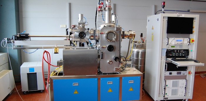
Many modern devices rely on structures composed of thin films, which enable researchers to engineer materials and electronic properties at nanometer length scales. The thin-film deposition lab provides the tools required to fabricate these layers with controlled thickness, uniformity, and composition.
Our lab specializes in physical vapor deposition (PVD) methods, particularly:
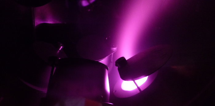
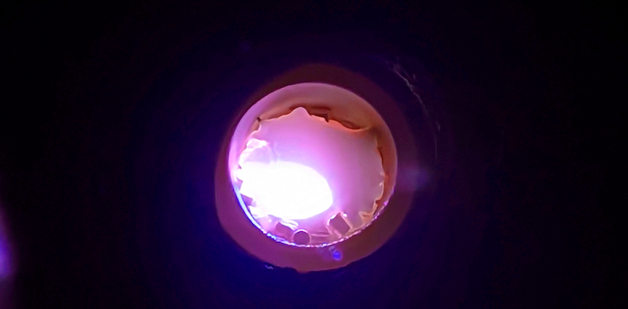
Sputtering, ideal for depositing metals, magnetic materials, superconductors, and complex alloys.
Thermal and electron-beam evaporation, allowing precise deposition of materials with excellent purity.
These techniques support research in quantum materials, superconducting devices, magnetism, van der Waals heterostructures, and other cutting-edge fields. The facility is accessible to students, researchers, and start-ups who require reproducible and high-quality thin films for their experiments and prototypes.
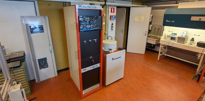
The deposition labs are located on the 6th floor of the Huygens building, in the Faculty of Science.
Guest users (for commercial use) can also use the equipment in the thin-film deposition lab. For further details, contact Marcel Hesselberth.
Students and employees can use the systems in the thin-film deposition lab for nano-fabrication if they have completed the relevant trainings for each system. For sputtering systems, contact Sander van Leeuwen, and for evaporation systems, contact Luc Wigbout.
© LION NanoLab
The facilities of Leiden NanoLab are part of Leiden Institute of Physics (LION) at Leiden University