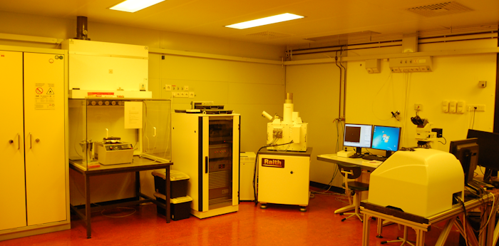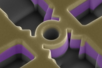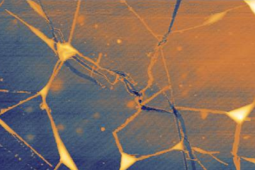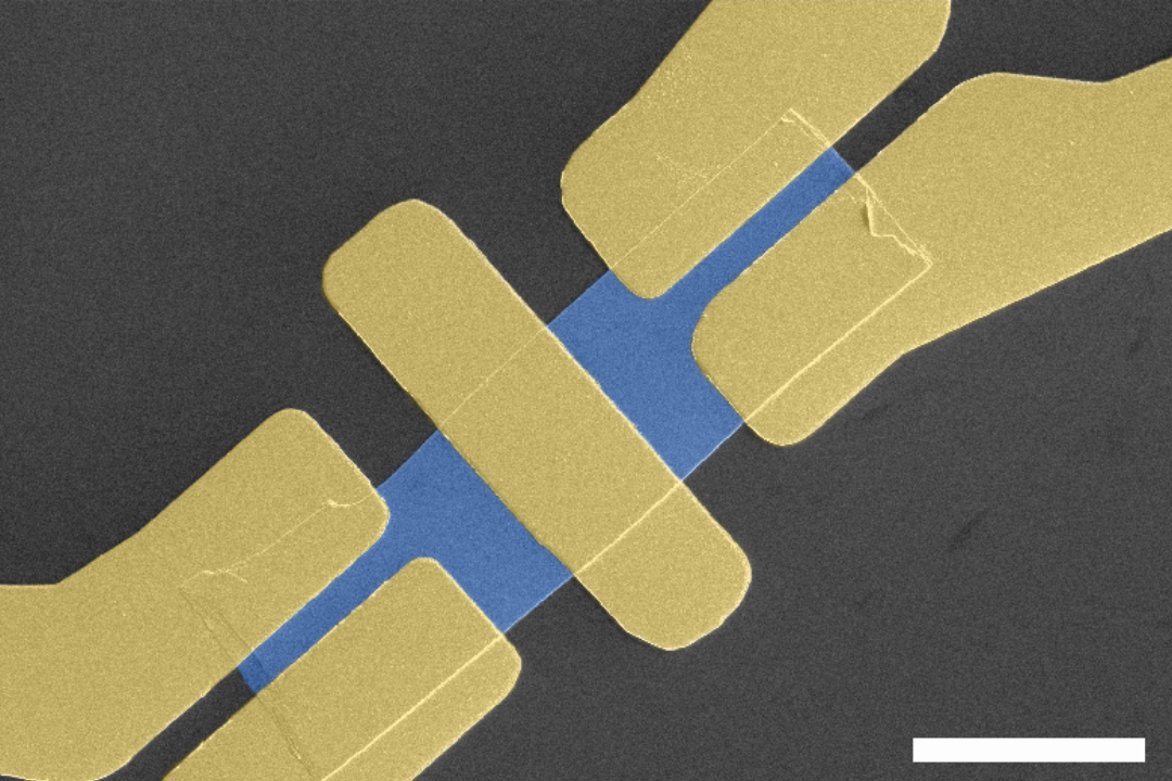
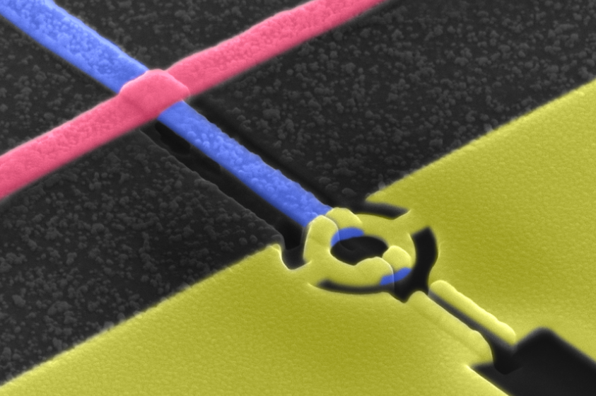
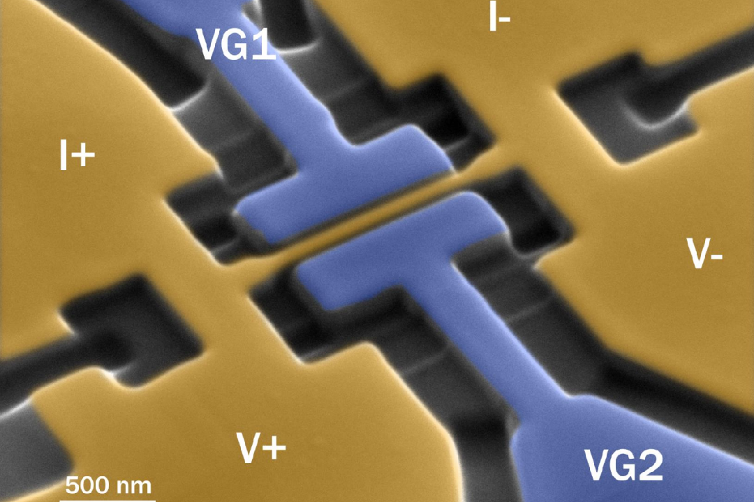

The Leiden NanoLab is a state-of-the-art facility for the fabrication and characterization of submicron and nanoscale devices. Our lab supports research and development involving a.o. magnetic materials, superconductors, and van der Waals-materials
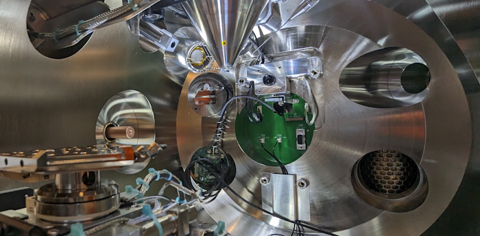
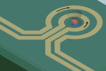
A dedicated part of the Leiden NanoLab operates under Class 10,000 cleanroom conditions, enabling high-precision lithography and related fabrication processes. To translate lithographically defined patterns into functional devices, we offer a set of thin-film deposition techniques and dry and wet etching methods.
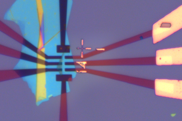
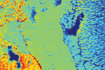
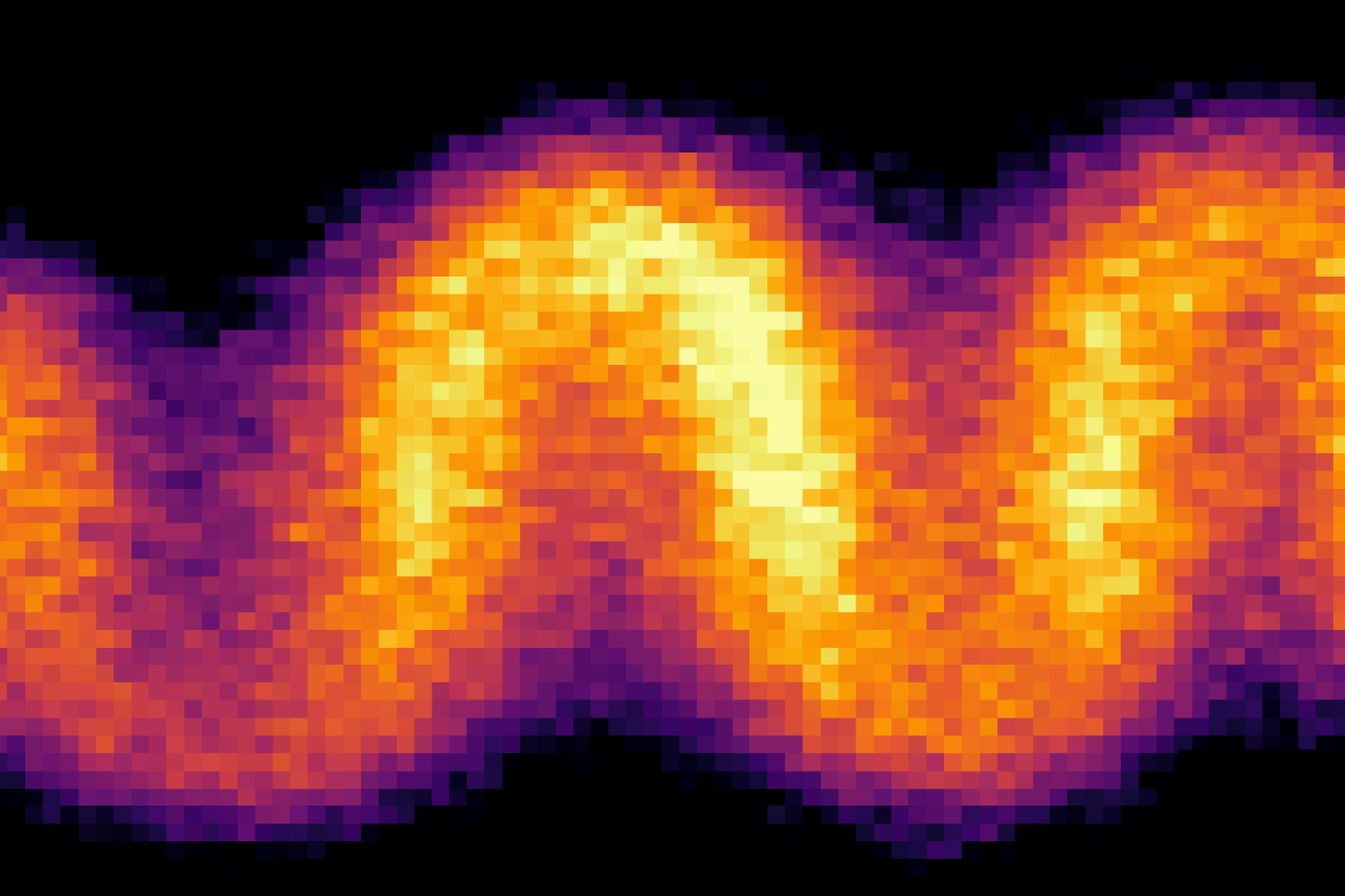
For device inspection and material analysis, the NanoLab provides a wide suite of characterization equipment, including Scanning Electron Microscopy (SEM) and Energy-Dispersive X-ray Spectroscopy (EDX). This combination of fabrication and characterization capabilities allows users to prototype, refine, and validate advanced nanoscale structures within a single facility.
With its broad equipment portfolio and experienced technical support, the Leiden NanoLab offers a flexible and accessible working environment for bachelor and master students, PhD candidates, postdoctoral researchers, university staff, and external partners.
The Leiden NanoLab is closely integrated with the experimental physics research groups of the Leiden Institute of Physics (LION). Researchers from these groups, as well as collaborators from other institutes and universities, make extensive use of the facility for cutting-edge experimental work.
In addition, start-ups and industry partners are welcome to access the NanoLab for research, prototyping, and product development in fields such as nanotechnology, quantum materials, and microfabrication.
To explore our available instruments, services, and access procedures, please select the facility or interest.
© 2025 LION NanoLab
The facilities of Leiden NanoLab are part of Leiden Institute of Physics (LION) at Leiden University