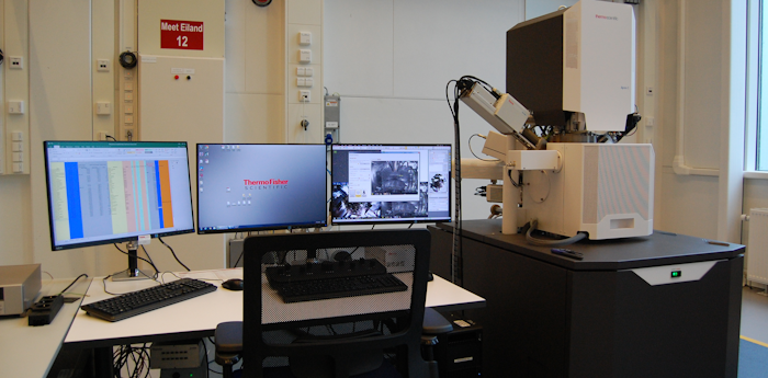
The electron microscopy lab provides essential tools for imaging, analyzing, and modifying nano-fabricated devices. Because the structures created in the Leiden NanoLab are far smaller than the resolution of optical instruments, electron microscopy techniques are crucial for understanding device morphology, composition, and fabrication quality.
Our facility includes high-resolution methods such as:
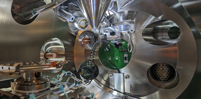
Scanning Electron Microscopy (SEM) for structural and morphological characterization.
Energy-Dispersive X-ray spectroscopy (EDX) for local compositional analysis.
Beyond characterization, the microscopes also support advanced capabilities, including:
Electron-Beam-Induced Deposition (EBID) for highly localized material deposition.
Focused Ion Beam (FIB) milling for precise patterning, thinning, and sample preparation.
These versatile tools make the Electron Microscopy Lab valuable not only for analysis but also for device repair, prototype refinement, and nanostructure engineering. The facility welcomes students and researchers from LION as well as external users working on nanoscale materials and device technologies.
The electron microscopy labs are located in the Ultramicroscopy Hall in the Gorlaeus building, in the (new) Faculty of Science.
External users (for commercial use) can also use the electron microscopy lab. For further details, contact Marcel Hesselberth.
Students and employees can use the systems in the electron microscopy lab for characterization of nano-fabricated samples if they have completed the relevant trainings for each system. For the aforementioned coating systems contact Sander van Leeuwen, for SEM/EDX, contact Luc Wigbout, for EBID, contact Marcel Hesselberth and for FIB, contact Kaveh Lahabi.
© LION NanoLab
The facilities of Leiden NanoLab are part of Leiden Institute of Physics (LION) at Leiden University